4-bit counter with optional enhancements
| ✅ Paper Type: Free Essay | ✅ Subject: Engineering |
| ✅ Wordcount: 833 words | ✅ Published: 12 Oct 2021 |
ABSTRACT
Automated placement systems often need a down counter for their services. The designing steps of counter for the control of individual terminals and precise logic sequence is very much important. In this article we will describe the logic diagram and architecture method for a synchronous binary counter. Our main aim of this writing is to include a modern low power approach, because MOSFET’S properties according to topology is really a challenging analysis. So in order to minimalize the power dissipation of circuit, we have utilized a number of stages in design process of architectural level and device level approach. After the amendments, as the chip are per gate is increasing continuously, at the same time switching frequency of gate remains same, and power losses are increased. So as a result it is more difficult to handle the heat because it becomes so expensive. In order to control the electricity dissipation, there are several alternative solutions used at each intellection level.
Introduction
Designing of digital circuits in logical manner like counter is really crucial because we have to ensure that counter is exactly working at the required rate of clock. So we have design the circuit in such a way that our delay will appear on exact timing.
Part of the design process is to optimize the counter and different architectures areas that are researched to choose the one that is suited to complete the function required. At that time circuit analysis plays the main role in order to proof the counter’s performance and function. In order to find the number of stages for the pipelines we have to determine the architecture of counter circuit first. It is efficient if our circuit will be in most optimized condition, considering all the objectives are achieving. As we all know fast circuits are used to do fast calculation because they have the most optimized design in order to avoid any sort of delay. Small circuits usually have less number of input and outputs so that is why the demand of power efficient circuits are increasing. Power dissipation Circuit size, writing complexity and circuit speed are the main recital requirements for logic design. As we all know that cell based designs are mainly depend on standard gates and smooth usage. Innovative logic styles are the best way to achieve high speed objectives. But due to high node and large clock load activities we don’t used it for low power circuits. As we will achieved the accurate digital working, our next target will be the high speed. Actually circuits are design with the delay based operation because if we will not encounter it our system will not work. Optimization of circuit is an achievement but it is not compulsory for the circuit. Reliability problems and area of implementation are also two important factor in circuit designing.
A flip-flop is a sequentially logically operated basic memory device which operates with two states. Actually flip flops are bi-directional memory element device which always work with the clock operation (synchronous). There are usually two outputs found in flip flop, first is for the normal operation and other is for the complementary operation. Digital data transfer and storage is done by flip flops, also it is utilized in registers as a banks for the numerical data. Flip flops are also used in the designing of counters. There are mainly two types found on the basis of application first is synchronous and other is a-synchronous. In synchronous counter the output is got switched by the clock pulse which is being applied from single clock at the same time. But in the a-synchronous counter the clock is provided from the output of former stage element. In this way the output ripple appear at the final count after passing from each stage.
In this report first we have assembled a 4 bit binary counter by using GDI technique with basic sequential elements like XOR gate and D flip flop.
Portion 2 will contain GDI technique consist of XOR gate and three T flip flop made of D flip flops.
Portion 3 will contain the 4 bit binary counter design which is proposed from T flip flop cells and AND gates.

Figure (1) diagram of 4-bit asynchronous counter
The figure showed the diagram of asynchronous 4-bit counter using D flip-flop.

Figure (2) the truth table

Figure (3) Schematic diagram of 4-bit counter
Design:


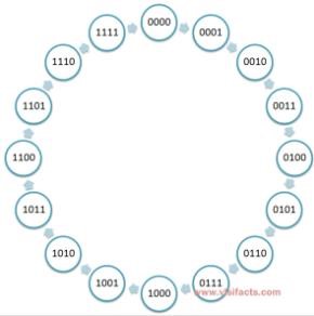
Figure (4) the state diagram of the 4-bit up counter
Conclusion
In this work we have designed a 4bit binary counter circuit with three T flip flop by using XOR gate,
D flip flop, AND gate and GDI technique. The designed counter is based on the 3V power supply only. After achieving higher output signal values and low power consumption we can say our design is mainly focusing on the qualitative design constraints. This design is quite better than the formerly made 4-bit binary counters.
References
1-Shreyaansh Srivastava Department of Electronics & Communication Engineering Northern India Engineering College, FC-26, Shastri Park, New Delhi 110053, India.
2- http://www.vlsifacts.com/circuit-design-4-bit-binary-counter-using-d-flip-flops/
Cite This Work
To export a reference to this article please select a referencing stye below:
Related Services
View allDMCA / Removal Request
If you are the original writer of this essay and no longer wish to have your work published on UKEssays.com then please click the following link to email our support team:
Request essay removal


